Introduction: The quality of transmission electron microscopy (TEM) lamella preparation directly determines the accuracy and reliability of semiconductor characterization, metrology, and failure analysis data. This article examines the key challenges and solutions in creating high-quality TEM samples for advanced semiconductor applications.
Why is TEM sample quality so critical now?
The semiconductor industry faces several technological inflection points requiring superior TEM analysis:
- Logic devices
- Gate-all-around (GAA) structures with 2 nm line widths
- Complex 3D architectures with buried features
- Increased difficulty in defect detection
- Memory technologies
- High-density, high-aspect-ratio channels
- Shrinking feature sizes
- Challenging defect visibility
- Power semiconductors
- Integration of SiC and GaN substrates
- Atomic-scale defect detection requirements
- Complex yield optimization needs
What are the three main challenges in TEM lamella preparation?
1. FIB damage control
- Amorphous damage increases proportionally with beam voltage
- Critical threshold: ~1 nm damage per kV
- Impact: 20 kV process creates 40 nm total damage zone
- Solution: Low-voltage (500 V) polishing capability
 demonstrating impact on sample quality.")
Figure 1: Comparison of ion beam damage at varying voltages (5 kV to 500 V) demonstrating impact on sample quality.
2. Precise cut placement
- Target accuracy requirements at nanometer scale
- Impact of misalignment on feature visibility
- Need for real-time monitoring and adjustment
- Importance of high-quality SEM imaging

Figure 2: Impact of cut placement accuracy: Off-center vs. centered fin structure in gate.
3. Lamella thickness control
- Feature size considerations
- Sub-10 nm thickness requirements
- Impact on artifact prevention
- Relationship to data quality

Figure 3: Thickness effect comparison: 16 nm vs. 7 nm sample showing artifact reduction.
How does sample preparation method affect results?
Traditional top-down method:
- Limitations for sub-30 nm samples
- Curtaining effects from dissimilar materials
- Challenges with final polishing
- Limited success with ultra-thin samples

Figure 4: Top-down preparation limitations showing curtaining effects.
Inverted sample preparation:
- Enables sub-10 nm sample creation
- Reduces curtaining artifacts
- Improved structural stability
- Automated process availability
Best practices for high-quality TEM lamella:
- Voltage selection
- Use lowest practical voltage for final polishing
- Monitor imaging quality during preparation
- Adjust parameters based on material properties
- Placement control
- Utilize orthogonal viewing capabilities
- Implement regular progress checks
- Maintain precise endpoint control
- Thickness management
- Choose appropriate preparation method based on target thickness
- Consider structural stability requirements
- Use wedge milling for ultra-thin samples

Figure 5: Inverted preparation method demonstrating improved sample quality and control and lamella end view for target verification.
Technical specifications and solutions
The Thermo Scientific Helios 6 FIB-SEM offers:
- Voltage range: 30 kV to 500 V
- 500 nm resolution at 500 eV
- Automated sample preparation via Thermo Scientific AutoTEM 6 Software
- High-precision cut placement capabilities
Things to remember
- Sample quality directly impacts data reliability
- Sub-10 nm samples require specialized preparation techniques
- Advanced automation tools improve success rates
- Low-voltage capabilities are essential for damage minimization


Removing Large Volumes of Material Fast with FIB-SEMs
Focused ion beam scanning electron microscopes (FIB-SEMs) ar...
Read More
Transmission Electron Microscopy in Semiconductors: Generating Ground Truth Insights
What is the current state of TEM in semiconductor analysis? ...
Read More
Physical and Electrical Failure Analysis of Power Semiconductor Devices
World energy consumption is expected to grow by nearly 50% b...
Read More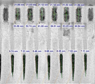
Revolutionizing the way TEM metrology data is collected
As I discussed in my 2024 year-end article, the semiconducto...
Read More
Leave a Reply